Pcb Design Tutorials
•build bill of materials with components supplier. Most manufacturers use metric size drills, so specifying imperial size holes really is counterproductive and can be prone to errors.

Embedded System Engineering Altium Designer Tutorial 4
If this panel is not displayed, select files from the system button at the bottom right of the main design window.

Pcb design tutorials. This pcb tutorial shows you how to get started on a new design, using the new board wizard to set up the initial board parameters. Click on this icon to run the software. Schematic capture and pcb layout from i.ytimg.com paid classified ads in bangor, portland, augusta,waterville, aroostook, penobscot, piscataquis, somerset, hancock, washington, maine.
Step by step pcb designing tutorial: You'll have access to multiple tutorials to help you gain a better understanding of advanced features as you venture deeper into pcb design. Pcb design tutorial by david l.
Translate to pcb (part 6) The wire that connects between the top layer and the bottom layer is called a via. There are many software available for pcb designing like orcad, eagle, express pcb.
Students will learn basic terminologies related to pcb's. Traces 12.5 resistance of conductors 12.5 voltage drop in signal leads—kelvin feedback 12.7 signal return currents 12.7 ground noise and ground loops 12.9 ground isolation techniques 12.11 static pcb effects 12.15 Pcb design tutorial pcb layout pcb basics.
When designing a 2 layer pcb we can connect the wire that are on the top layer and the bottom layer. •design schematic •design pcb layout and routing. Alternatively, you could select printed circuit board design in the pick a task section of the
Produce gerber, drill and pick and place files for manufacturing your pcb. Summary: in this pcb design tutorial, i have explained all the major steps to design a pcb with diptrace. 09.01.2020 · cadence design entry hdl 使用教程前言cadence design entry hdl是cadence内部集成的一款板级的eda设计工具.
It is considered that you have installed the software and have basic knowledge of electronics. Designspark pcb in 3 minutes and 42 seconds. •most important step in designing a pcb.
Creating a new pcb layout, syncing a schematics with pcb layout, and setting up design rules. Hi, welcome to this free altium designer tutorial for beginners series. And i have used all the free resources to design the pcb.
Wizards (part 4) designspark pcb basic course: Draw and modify component footprints. Schematics (part 5) designspark pcb basic course:
Integrated 3d modeling for printed circuit board design makes altium designer stand out from the rest. I have covered how to draw schematics, routing the board, generating gerber files for manufacturing the pcb. Over the next few pages, we'll discuss the composition of a printed circuit board, cover some terminology, a look at methods of assembly, and discuss briefly the design process behind creating a new pcb.
Placing components on pcb pcb design (with eagle tutorial) ta: Select file » new » project » pcb project from the menus, or click on blank project (pcb) in the new section of the files panel. In these video tutorials you will learn how to make it in proteus ares software.
Libraries (part 2) designspark pcb basic course: Jones page 5 of 25 5 you will find that many pcb manufacturers will follow these basic guidelines also, for when they ask you to provide details for a quote to manufacture your board. In this final section on pcb layout, we're going to look at reduced schematics from the.
Familiarisation (part 1) designspark pcb basic course: Printed circuit board (pcb) design issues introduction 12.1 section 12.1: Pcb design tutorial pcb layout circuit diptrace pcb.
The free, open source software allows you to create pcb layouts and schematics. •be aware of package size/code. How to cover vias with solder mask in eagle.
Creating components (part 3) designspark pcb basic course: 2 layout design tutorials moving the. • now you know how to layout a pcb.
This tutorial will breakdown what makes up a pcb and some of the common terms used in the pcb world. (in our example, we will use the led flasher circuit and design its pcb). But if you are beginner in designing, i recommend you to use proteus ares.
Video tutorial on pcb designing using proteus ares : I'm using version 20.2.5follow along with this pcb design tutorial for beginners usin.

Multilayer pcb design tutorial altium
Altium Designer Tutorial Deutsch PCB Circuits
Zuken Pcb Design Tutorial PCB Circuits


KiCAD PCB Design Tutorial Part 1 Start a new project

Altium Designer Tutorial Pcb Design Fundamentals PCB
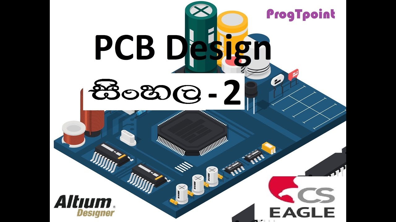
PCB Designing Sinhala Tutorial 2 Schematic Design YouTube

PCB Design Sinhala tutorial 3 Designing PCB layout YouTube
Basic PCB designing in EAGLE Part 1 YouTube
eagle pcb design software tutorial projectiot123

An Introductory Multilayer PCB Design Tutorial Advanced
Do It Yourself Tutorials PCB Design Tutorial 17 for

Pcb design tutorial । Pcb design tutorial for beginners
Multisim Pcb Design Tutorial Pcb Circuits

PCB DESIGN tutorial part 1മലയാളത്തിൽ YouTube

High speed pcb design OrCAD
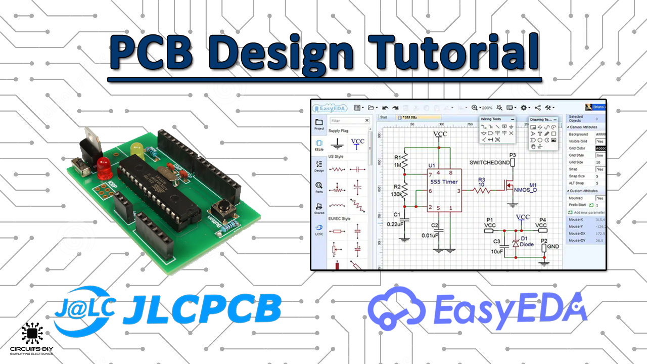
PCB Design Tutorial Using EasyEDA & JLCPCB PCB Designing

EAGLE PCB Design Tutorial found on Tutorials

Pads pcb design tutorial
Cadence PCB Design 2020 and Options CB Distribution